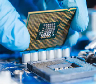
A new Chinese lithographic scanner uses a light wavelength of 193 nm and can print chips with a resolution of 65 nm . This resolution was available to customers of the Dutch company ASML as early as 2009.
China's Ministry of Industry and Information Technology suggests that the country is 15 years behind the US in microcircuit production. This is, in particular, about the company ASML, writes WCCFTech resource.
Due to recent sanctions by the Dutch government requiring ASML to obtain licenses before selling obsolete DUV-based chip manufacturing machines, China has developed its own DUV scanner. A document on the implementation of the guidelines says that Chinese scientists have created an argon fluoride-based lithography machine with a layer thickness of less than 8 nm. This lithographic scanner uses a light wavelength of 193 nm and can print chips with a resolution of 65 nm. This resolution was available to customers of the Dutch giant back in 2009.
If we talk about the latest ASML product portfolio, the closest analogue is the TWINSCAN XT:1460K scanner. This machine also has sub-65nm resolution and uses a 193nm argon fluoride light source. However, it is still more advanced than the Chinese machine, as the overlay specification is less than 2.5nm, which is far superior to the 8nm overlay claimed by the Chinese ministry.
200% Deposit Bonus up to €3,000 180% First Deposit Bonus up to $20,000Since semiconductor manufacturing involves the manipulation of light to print the smallest circuits on a silicon wafer, its quality and technical parameters include the manipulation of light. The resolution of a chip machine is simply defined as the minimum feature size that the machine can print. This size depends on many other factors, the most important of which are the numerical aperture of the machine, its depth of focus and the size of the mask.
In these cases, a higher numerical aperture usually means a lower resolution, allowing chip makers to reduce chip sizes. Overlapping the machine — it is her ability to apply new patterns to existing patterns on the plate. Since chip manufacturing uses a mask to imprint the circuit patterns for electrical conductivity, machines with lower overlay capabilities are better because they allow the circuits to be packed tightly.
ASML first introduced its TWINSCAN chip machines in 2005. Since then, the firm has moved on to immersion machines and new EUV tools, which are gradually becoming the backbone of the industry. Its TWINSCAN:XT 1460 scanner, which is the closest approximation to the currently available TWINSCAN:XT:1460K machine, first appeared in the firm's 2015 annual report with a resolution of 65 nm and a light wavelength of 193 nm.
Chip machines have become a valuable commodity for the PRC, as the latest equipment is manufactured only by ASML. At the same time, local Chinese equipment can help the country reduce its dependence on Western products. This is important for development in a strategic industry in an era where AI software requires the latest semiconductors for maximum performance.
Regarding the document, it outlines three key details of China's latest DUV lithography machine: resolution, wavelength and overlay . The scanner is a machine based on argon fluoride, which has been used in the global semiconductor industry for about two decades.

